

Choosing a stackup
Understand how layer arrangements affect signal integrity, return paths and routing.
Read the guideTHE SIX-LAYER DESIGN RESOURCE
Understand your stackup, define your requirements, and prepare your next build.
DESIGN / VERIFY / MANUFACTURE / WITH CONFIDENCE
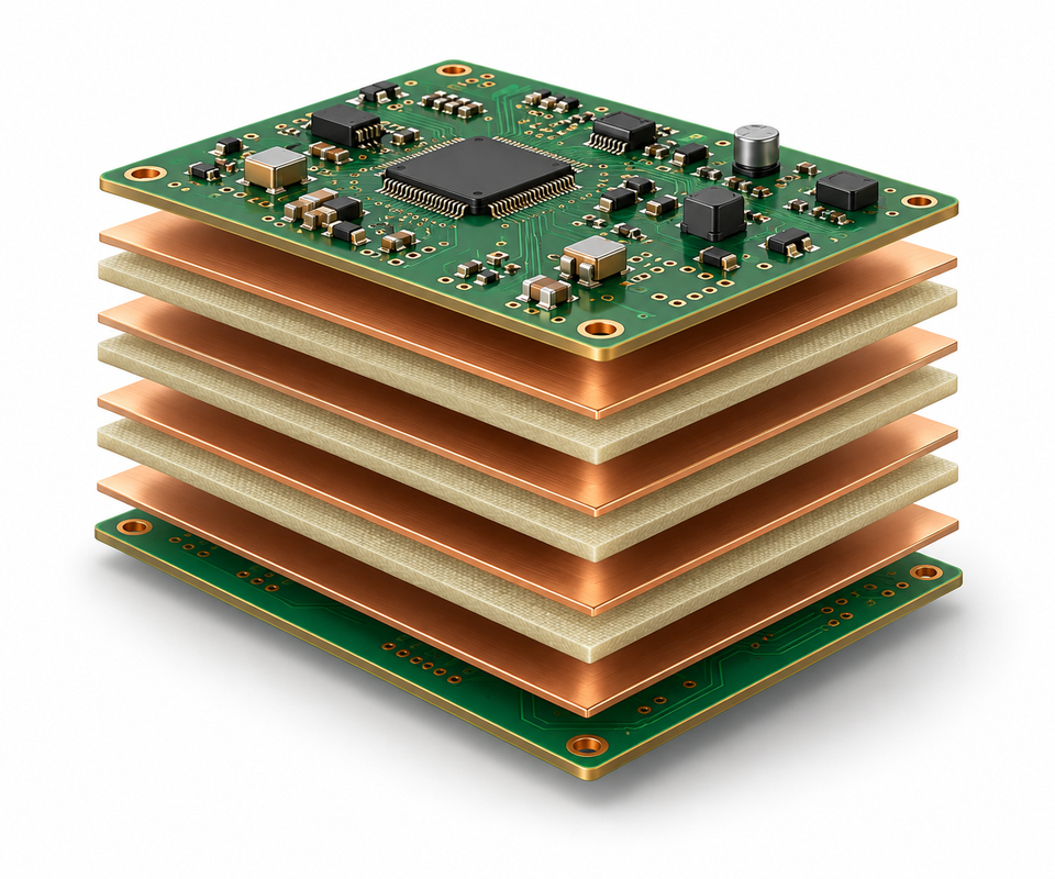
Answering a few questions early helps you create a clearer path from electrical intent to fabrication.
Plan continuous reference planes and check how return current crosses layer transitions.
Assign signal and plane functions to match routing density and power needs.
Confirm dielectric and copper construction before finalizing controlled traces.
A laminate choice needs to match electrical, thermal and mechanical requirements.
Consider assembly reflow and the operating environment as separate conditions.
Use material data at the relevant frequency and test method.
Confirm available cores and prepregs before fixing your dielectric dimensions.
Impedance is a result of the complete transmission-line geometry, not the layer count.
State each controlled net class and the required measurement conditions.
Record trace width, spacing, dielectric height and copper thickness.
Agree any coupon requirements and the reporting needed for acceptance.
A complete handoff reduces questions that can delay a build.
Supply a readable copper layer map, outline and plated / non-plated drills.
Identify material, finish and construction constraints in the fabrication notes.
Specify dimensional, electrical and documentation requirements before release.
MAKE INFORMED DECISIONS
Understand how layer arrangements affect signal integrity, return paths and routing.
Read the guide
Get your design ready with a clear layer map, drill data and fabrication notes.
Read the guide
See how geometry, materials and manufacturing choices shape project cost.
Read the guideSPECIFY WHAT MATTERS
Six copper layers make room for routing and reference planes. A manufacturable board also needs an agreed material, dielectric construction, hole structure and acceptance criteria.
Explore manufacturing capabilities| Layer construction | Six conductive layers with a clearly identified layer order |
|---|---|
| Base material | Laminate family, Tg and electrical requirements |
| Board thickness | Finished thickness and mechanical tolerance |
| Copper | Starting and finished copper requirements by layer |
| Impedance | Target, tolerance, trace geometry and reference layers |
| Finish & holes | Surface finish, plated / non-plated drill data and via requirements |
| Delivery | Quantity, prototype or production intent, and required date |
Material availability, geometry and delivery are reviewed together for each project.
A CLEAR PATH TO PRODUCTION
Send Gerber files, drill data, quantity and the specification you need.
Resolve layer order, materials, impedance and fabrication questions.
Agree the technical scope, acceptance requirements and delivery plan.
Use the approved fabrication package as the controlled build reference.
BALANCE PERFORMANCE & PRACTICALITY
A stackup is more than a layer count. Compare electrical, mechanical and procurement requirements before committing to a build.
Discuss your requirementsMatch laminate properties to operating conditions, assembly temperatures and electrical needs.
Consider pad flatness, storage, solderability and the assembly process.
Material availability, review cycles, special processes and shipping all affect the schedule.
Specify the inspection evidence, acceptance criteria and traceability the application needs.
DESIGN AROUND THE APPLICATION
Plan robust return paths, power distribution and environmental requirements.
Discuss this applicationDefine interface constraints, impedance targets and signal routing priorities.
Discuss this applicationBalance board size, power integrity, antenna keep-outs and production cost.
Discuss this applicationCOMMON QUESTIONS
Start with the decisions that make a quotation more useful.
It is a circuit board with six conductive copper layers separated by dielectric material. Those layers can carry signals, power or reference planes; their functions depend on the design.
No. Choose the layer arrangement around return paths, routing density, power distribution and the manufacturer’s achievable construction. Confirm dielectric thicknesses before routing impedance-controlled signals.
A complete Gerber set, drill files, an outline and fabrication notes provide a useful starting point. Include quantity, material, finish, impedance requirements and the required date. Assembly inquiries also need a BOM and placement data.
RAR is supported alongside ZIP, 7Z, documents, images and common PCB engineering files. Check the enabled formats on the inquiry form. You can attach up to five files, 10 MiB per file and 25 MiB in total.
A firm plan depends on material availability, construction, special processing and order quantity. Share your target date so those factors can be reviewed together.
No. Layer count alone does not ensure performance. Continuous reference paths, geometry, placement and appropriate routing rules remain essential.
FROM DESIGN TO REALITY
Share your requirements and optional supporting files.